


Low noise block (LNB) is a critical functional block in the receiver chain of satellite communication systems. An LNB basically consists of a low noise amplifier (LNA) chain and a frequency down-converter. While the components and circuitry used in LNBs have evolved over time and vary considerably among products, the basic requirement for the LNA remains the same, that is, providing the lowest possible noise figure with an adequate matching condition at the amplifier input.
This technical note discusses some design considerations for an ultra low noise amplifier intended as the first stage LNA of satellite receivers. The chosen frequency is 12GHz which is at the lower end of Ku-band and is widely used in high data rate satellite communication applications owing to its desirable balance among three key system performance parameters: (1) available bandwidth (~ 500MHz), (2) microwave propagation characteristics (rain fade becomes more severe as frequency further increases), and (3) required antenna size (which is roughly scaled with frequency). The discussion is provided at high level for general information. Actual designs require much more in-depth knowledge and expertise in the product development.
DEVICE
The device discussed in this note is CEL’s low noise transistor CE3512K2. It is manufactured using the state of the art GaAs pseudomorphic high electron mobility transistor (pHEMT) technology which offers a superior noise performance. In addition, the CE3512K2 employs a hollow air cavity package structure which eliminates significantly the RF power loss associated with packaging materials. To keep the device cost consistent with commercial applications, the cavity package of the CE3512K2 is non-hermetically sealed. For this reason, a non-cleaning flux soldering process is recommended for PCB assembly (for details, see K2 & K3 Package Devices Recommended Soldering Flux & Cleaning Conditions). As an alternative, the CE3514M4, which utilizes molded plastic package, does not require non-cleaning flux. Its noise figure is slightly higher than that of the CE3512K2.
The CE3512K2 is designed for Ku-band LNA applications. It also exhibits excellent phase noise characteristics when used in oscillator designs at higher frequencies. A typical example is 24GHz oscillator in Doppler radar applications.
BIAS CIRCUITS
Figure 1 shows a typical biasing scheme for a field-effect-transistor (FET) used in RF amplifiers in the GHz range. Only the bias circuit for the drain needs to be considered since the gate is a high impedance state at DC. The inductance value is usually chosen high enough to provide sufficient RF isolation at the operation frequency, although in some cases the inductor in the bias circuit can also be part of matching network. The shunt capacitance provides a low impedance point, functioning as a low pass filter to the noise and other unwanted signals from the DC power supply. As frequency increases the parasitic effects in both inductors and capacitors become dominant. As a result, for an amplifier operating above 10GHz, transmission-line based components are often used in both bias and matching circuits.
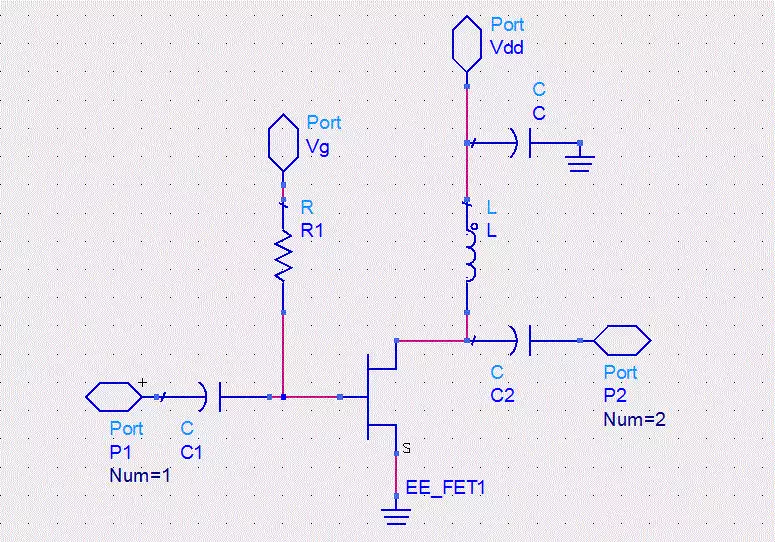
Figure 1
Typical L-C bias circuit for a FET (matching networks not shown)
It is known that a quarter-wavelength (denoted as λ / 4 ) transmission line transforms a short circuit to an open. This characteristic is utilized in bias circuit designs where a λ / 4 transmission line is implemented to replace the inductor for RF isolation. In principle, there is no low-frequency limit for this technique. In practice, however, it is usually employed in circuits operating at high gigahertz and above due to the PCB size constraint. For the shunt capacitor, there are two common transmission-line implementations, namely rectangle and radial open stubs. The action of a rectangle stub can be understood using the same concept of impedance transformation through a λ / 4 transmission line. In this case, an open is transformed to a short. Analysis of a radial stub is much more complex. Practically, the required length (the radius) of a radial stub is shorter than the rectangle counterpart for the open-to-short transformation. In addition, the low impedance point is well defined in the case of radial stub because of its narrow width at the interface with the through transmission line. We will use a radial stub to illustrate the circuit performance in this note.
DC BLOCKING CAPACITORS
Like in any transistor circuit, a DC blocking capacitor is generally required at both the input and output of the CE3512K2 amplifier circuit. At 12GHz, a typical chip capacitor has two undesirable effects: 1) The insertion loss of the input capacitor, which can be as high as a fraction of dB, directly degrades the noise figure by the same amount; 2) The parasitic effects of the capacitor complicates the matching network design. While special high frequency capacitors, designed to minimize these effects, are available, they are generally costly. For LNB applications, fortunately, the input DC blocking capacitor is not needed because the LNA circuit usually interfaces with a waveguide component that is naturally DC isolated. At the output side, a transmission-line based bandpass filter is often employed for out-of-band noise rejection. This type filter circuit is usually DC isolated as well, eliminating the need for a DC blocking capacitor. In the case when such a filter is not practical or required, a series capacitor at the output has little impact on the circuit performance, and is therefore acceptable.
In prototyping stage, a circuit without DC capacitors imposes an issue on noise figure measurement (maybe on S parameter measurement as well) because the measurement instrument is usually DC coupled. A common practical solution is to insert a DC blocking component or a bias-tee between the DUT and the instrument. The noise figure of the DUT then can be estimated by subtracting the insertion loss of the input DC block from the measured noise figure. Note that this procedure only corrects the effect of the DC block in magnitude. The measurement uncertainty associated with the phase variations remains. A more sophisticated process that involves phase calibration can be implemented if more accurate measurement results are required.
MATCHING CIRCUITS
In the design of an LNA input matching network, it is known that a perfect input return loss and the minimum noise figure ( NFmin provided in the S parameter file) generally cannot be achieved simultaneously. A typical procedure for a commercial product is first determine the minimum specification for the return loss (10dB is generally considered acceptable) and then design the matching to achieve the best possible noise figure under the return-loss specification. For the CE3512K2, the two matching points, for return loss and noise figure respectively, turn out to be remarkably close at 12GHz, as evidenced in Figure 3. This is not a coincidence, since the device is specifically designed for this band.
For frequency above 10 GHz, matching networks usually only consist of transmission line components, typically series transmission lines and open stubs. Multiple stubs can be employed for improved frequency response in bandwidth.
SIMULATION RESULTS
A design in practice normally starts with a simulation using the noise and S parameters, then followed by a bench tuning to optimize the performance.
Figure 2 shows the schematic for a 12GHz LNA using the CE3512K2. The design incorporates these considerations discussed above. The simulation results for gain, S21, input and output return losses, S11 and S22, and noise figure are shown in Figure 3. Note that the design has achieved a good input return loss while the noise figure is only slightly higher than NFmin (by 0.02dB). At the output, a moderate S22 is achieved without any matching.
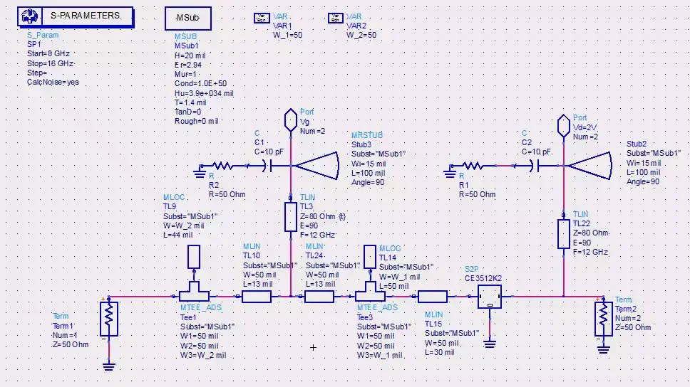
Figure 2
Simulation setup for 12GHz LNA using the CE3512K2
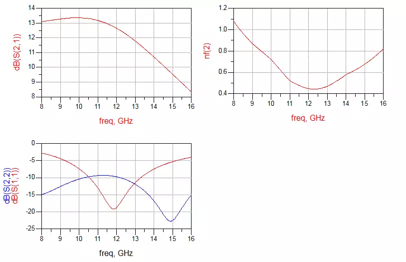
Figure 3
Simulation Results
In actual product development, the design process is much more complex due to various imperfection in components/devices and constraints on circuit implementation. While the simulation shows a noise figure of about 0.5dB, a product specification of 1dB or slightly lower for noise figure is generally considered excellent when everything is taken into account. Nevertheless the considerations outlined in this note are relevant in real world applications.